Thermal Grade
Thermal Super-material Diamond: Engineered for Extreme Heat Flux Management
Single Crystals & Polycrystalline Wafers Redefining Thermal Limits
Core Value Proposition
Deploy the world’s highest thermal conductivity material (2000+ W/mK) in scalable formats – from precision single-crystal heat spreaders to 4-inch polycrystalline wafers – solving thermal bottlenecks in power electronics, RF systems, and laser technologies.
Technology Comparison Table
| Property | Our Polycrystalline Wafer | Our Single Crystal Substrtes | Competitors (Cu/AlN) |
| Thermal Conductivity | 1000–1400 W/mK | >2000 W/mK | Cu: 400 W/mK · AlN: 180 W/mK |
| Max. Size | 4-inch (100 mm) dia. | 30×30 mm | Cu: 300 mm · AlN: 150 mm |
| CTE Match | 0.8–1.2 ppm/K (Si/GaN close) | 0.9 ppm/K | Cu: 17 ppm/K · AlN: 4.5 ppm/K |
| Dielectric Strength | >10 MV/cm | >10 MV/cm | Cu: Conductive · AlN: 1.7 MV/cm |
| Weight Savings | 65% lighter than copper | 70% lighter than copper | N/A |
Product Line Specifications
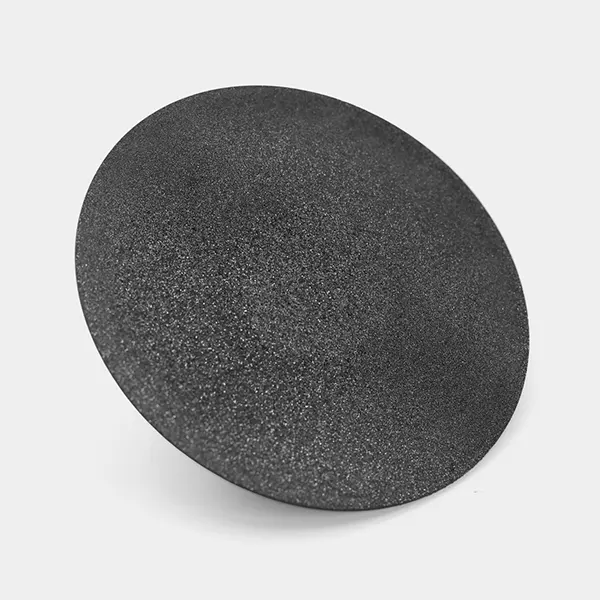
Polycrystalline Diamond Wafers
- Sizes: 25 mm → 100 mm (4″) diameter
- Thickness: 300 μm → 2 mm (±10 μm)
- Thermal Performance: 1000–1400 W/mK (verified laser flash analysis)
- Form : Self-Standing or Epitaxial on Si
Single Crystal Heat Spreaders
- Dimensions: Up to 30×30 mm(custom sizes available)
- Thickness: 200 μm → 12 mm
- Thermal Performance: >2000 W/mK
- Orientation: (100), (110) or any Intermediate orientation

- Thermal Conductivity up to 2000 W / mK
- Poly-crystalline wafers up to 4 inch Diameter (101.5 mm)
- Thickness: 0.1 mm up to 1 mm
- Surface roughness < 50 nm RA
Are you interested in Thermal Grade Management?
Solve Critical Thermal Challenges
GaN/SiC Power Electronics
Prevent GaN HEMT degradation at 1+ kW/cm²:
- Diamond submounts reduce ΔT by 60% vs. copper
- CTE match eliminates solder fatigue failures
5G/6G RF Amplifiers
Enable mmWave operation with diamond:
- 4-inch wafers integrate directly with GaN-on-SiC fabs
- 22× lower RF loss than Cu-Mo composites
High-Power Laser Diodes
Double output power with diamond heatsinks:
- 2000 W/mK single crystals for 500 W+ laser bars
- Transparency at pump wavelengths (808 nm) for edge-cooling
Why Diamond Outperforms
At >2000 W/mK, diamond conducts heat 5× faster than copper while being electrically insulating. Our materials deliver:
- Zero thermal runaway at 1000+ W/cm² flux
- 10× longer lifetime vs. AlN in power cycling tests
- Direct bonding to Si, GaAs, GaN without stress cracking
Manufacturing Advantages
Scalability
4-inch polycrystalline wafers enable:
- Standard semiconductor tooling compatibility
- Batch processing for volume production (Qty 1000+/month)
Reliability by Design
Grain boundary engineering for isotropic thermal flow
- XRD-verified crystal orientation in single crystals
- Laser-cut edges for crack prevention

Frequently Asked Questions (FAQs)
How much better is diamond at cooling than copper?
Diamond conducts heat 5× faster than copper (2000+ W/mK vs. 400 W/mK). It stays cooler under extreme heat, making it perfect for high-power electronics and lasers.
Can diamond replace copper in electronics?
Yes! Diamond cools better, weighs 70% less, and won’t expand/break like copper. It’s also electrically insulating, so it won’t short-circuit your devices.
What sizes do your diamond wafers come in?
We offer:
Polycrystalline wafers (4-inch/100 mm diameter) for large-scale cooling.
Single-crystal diamond (up to 30×30 mm) for precision heat spreading.
Why is diamond good for 5G and power electronics?
Diamond handles 1000+ W/cm² heat without failing, keeps GaN/SiC chips cool, and reduces RF signal loss 22× better than copper-molybdenum.
How do I test diamond for my application?
We provide thermal test reports (ASTM certified) and can help simulate how diamond improves your design. Ask for samples or our ROI whitepaper.
Transform Thermal Management
Request thermal simulation support for your module or download our whitepaper: ‘Diamond vs. Cu: ROI Calculation for Power Electronics’
